SELECTIVE HEAVY COPPER PLATING
Pro-Tech Interconnect Solutions is at the top of Innovation for PCB Heavy Copper Plating in developing heavy copper circuits - features of multiple copper heights on one board in addition, to its legacy products for computing, automotive, military, and industrial controls since 2002. Pro-Tech’s Team works diligently with its customers to fully understand new product designs. New designs are reviewed by our Senior Research and Development Team in CAM Engineers, Manufacturing Engineers and Sales Engineering teams to fully understand the manufacturing challenges. This allows detailed and timely communication back to the customer in the event there are any issues. Protech’s experience and comprehensive set of design rules lays the foundation for getting the product right the 1st time. Design Review Meetings are common place at Pro-Tech and viewed as a core competency to its business and customer service. Processes are managed to meet the demands of producing heavy copper PCB’S. Typical features- requirements include copper thickness, coplanarity, line width /spacing formation, vertical copper sidewall formation, solder mask coating thicknesses-encapsulation, heavy copper resin fill and drilled-routed features.
Thermal management
Isolated plate up for individual component cooling.
Full via copper fill stitching for thermal transfer of subsurface structures to surface or back plane heatsink.
Power/Current management
Selective trace/feature buildup to meet current flow requirements across PCB.
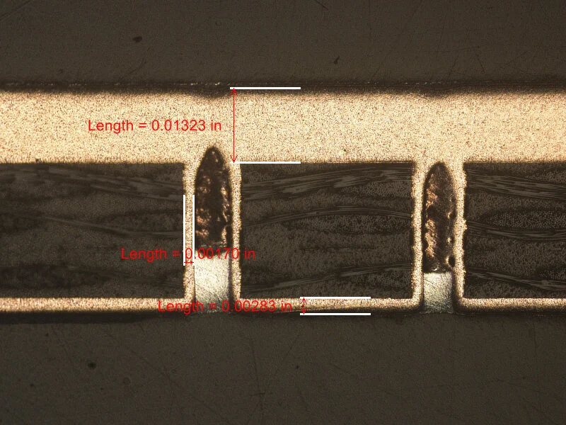
Signal/features internal and/or external can be any size as long as minimum of 1:1 ratio is maintained.
Selective PTH plate up for front to back current transfer.
PTH copper ranging from .0005” to .030”+
Reduced layer count due to increased inner layer plate up to handle increased current.
Inner layer copper ranging from .0003” to .160”+
Eliminate secondary heatsink bonding process.
Heatsinks can be selectively added during PCB manufacturing process to areas/components requiring additional thermal dissipation.

Create standoff structures for elevated component mounts.
Structures can be manufacturing into the PCB surface allowing elevated external connections or component mounts to be made without disruption too or reducing PCB functional surface area.
Elevated structures can be of any shape or form .001” to .100”+ in height.

10 oz. Cu plate up.

100 oz. Cu Selective plate up with adjacent 2 oz. Cu control circuits.

30 oz. Cu Selective plate up.

30 oz. Cu Selective plate up with adjacent 2oz. Cu control circuit.

Enhance PCB ridged strength.